contents | business | |||||||
| Toshiba Opens the New 200mm Wafer-Based Production Fab 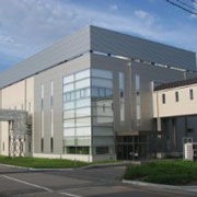 Toshiba and Kaga Toshiba have marked the official opening of a new semiconductor production fab based on 200mm wafers at Kaga Toshiba, a consolidated subsidiary of Toshiba based in Ishikawa prefecture, Japan. The new fab will enhance production capacity for power devices. Demand is growing for power devices that control current flow and voltage conversion in digital consumer products, including TVs and personal mobile equipment, and hybrid vehicles. Toshiba and Kaga Toshiba's investment in the new production fab will increase capacity for these key devices. Toshiba and Kaga Toshiba have marked the official opening of a new semiconductor production fab based on 200mm wafers at Kaga Toshiba, a consolidated subsidiary of Toshiba based in Ishikawa prefecture, Japan. The new fab will enhance production capacity for power devices. Demand is growing for power devices that control current flow and voltage conversion in digital consumer products, including TVs and personal mobile equipment, and hybrid vehicles. Toshiba and Kaga Toshiba's investment in the new production fab will increase capacity for these key devices.The new fab came on-line at the end of September, completing the first phase of an investment program in a new building and production equipment that is expected to be total 55 billion yen in the five years from FY2006 to FY2010. The new fab is planned to ramp up to 60,000 wafers a month, and capacity may be further expanded to meet market growth. Toshiba Group's semiconductor business covers three major product areas: system LSIs, memories and discrete devices. Kaga Toshiba operates as a key Toshiba Group facility for discrete devices, carrying out product development and front- and back-end processes for small-signal devices and power devices. write your comments about the article :: © 2007 Computing News :: home page |