contents | hardware | |||||||
| Elpida Rolls Out 70nm Process Technology DRAM 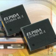 Elpida Memory has begun mass production of the DRAM industry's first 1-Gigabit and 512-Megabit DDR2 SDRAMs using 70-nanometer process technology. Elpida is currently realizing high yields and productivity from its 90nm process technology used in mass production. The technology that has made those achievements possible has been applied to the development of the more advanced 70nm process technology. A 1-Gigabit and 512-Megabit DDR2 SDRAM using 70nm process technology can be used in many applications, including high-end servers that need to process large amounts of data, high-performance mobile equipment, high definition digital TVs, next-generation DVD recorders, digital single-lens reflex cameras and other digital consumer equipment that must have advanced image processing capabilities. Elpida Memory has begun mass production of the DRAM industry's first 1-Gigabit and 512-Megabit DDR2 SDRAMs using 70-nanometer process technology. Elpida is currently realizing high yields and productivity from its 90nm process technology used in mass production. The technology that has made those achievements possible has been applied to the development of the more advanced 70nm process technology. A 1-Gigabit and 512-Megabit DDR2 SDRAM using 70nm process technology can be used in many applications, including high-end servers that need to process large amounts of data, high-performance mobile equipment, high definition digital TVs, next-generation DVD recorders, digital single-lens reflex cameras and other digital consumer equipment that must have advanced image processing capabilities.The 70nm process technology enables 800MHz and 1GHz speed functionality in combination with high-performance operations, but it also provides for a reduction in chip size allowing incrementally more chips per DRAM wafer which increases productivity and volume overall. Among 512-Megabit products, the technology has made possible the world's smallest chip size for a 512-Megabit DDR2 SDRAM. Production of DDR2 SDRAM using 70nm processing has already started, and the first product shipments are expected to begin in the first quarter of 2007. Elpida plans to make aggressive use of its new 70nm process technology in the production of Mobile RAM for mobile phones and other mobile equipment and in memory products used in high-end digital consumer equipment and across the entire server/PC market. write your comments about the article :: © 2006 Computing News :: home page |