contents | hardware | |||||||
| Renesas' Transistor Technology for 45 nm Node Generation Chips 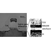 Renesas Technology has announced the development of a high-performance transistor technology for microprocessor and SoC (system-on-a-chip) products of the 45 nm node generation and beyond. The newly developed technology consists of high-performance CMIS transistors with a hybrid structure employing metal gates for p-type transistors and conventional polysilicon gates for n-type transistors. It can be implemented without making major changes to current fabrication processes, thereby lowering production costs. Renesas Technology has announced the development of a high-performance transistor technology for microprocessor and SoC (system-on-a-chip) products of the 45 nm node generation and beyond. The newly developed technology consists of high-performance CMIS transistors with a hybrid structure employing metal gates for p-type transistors and conventional polysilicon gates for n-type transistors. It can be implemented without making major changes to current fabrication processes, thereby lowering production costs.Prototype transistors with a gate length of 40 nm fabricated using the new technology exhibit excellent performance. Their drive capacity is the world's top level at 620 μA/μm for n-type transistors and 360 μA/μm for p-type transistors. In addition, reliability in terms of factors such as gate dielectrics strength has been confirmed to be problem-free, even with a newly developed production process flow. In recent years, as the age of ubiquitous networking approaches, there has been strong demand for many types of equipment offering a higher level of functionality and performance, as well as for mobile devices that can operate for long battery life. Advanced semiconductor devices are essential in order to make products combining high performance and low power consumption a reality. Ultrafine semiconductor fabrication processes provide a way to achieve enhanced functionality and reduced power consumption through high integration. However, as the trend toward ultrafine semiconductor fabrication processes advances, the gate dielectrics used in the transistors become thinner. This result causes a serious problem, such as increasing in gate leakage current due to the tunneling phenomenon. One effective solution is to use a high-permittivity dielectrics, a so-called high-k, on top of an oxide silicon film. However, using a high-k result in a phenomenon called "Fermi level pinning", which fixes the transistor's threshold voltage at a high level. The introduction of metal gates is an effective way to suppress this phenomenon, and it is thought that it will be essential in the 45 nm node process generation and beyond. For this reason, vigorous work is being done in the industry to develop dual-metal-gate transistor technology that combines high-k and metal gates and is suitable for both n-type and p-type transistors. However, these efforts face the following problems: 1) There are two types of transistors: 1. n-type transistors (which operate using electrons having a negative electric charge) and 2. p-type transistors (which operate using positive holes having a positive electric charge). This means that the metal gates must be made of two different materials, one suitable for n-type transistors and one suitable for p-type transistors. 2) If two materials are used, one for n-type transistors and one for p-type transistors, and the workability of the materials differs, separate dedicated fabrication equipment will be required for each. This will tend to increase the complexity and number of steps in the fabrication process, resulting in higher production costs. 3) There are also a number of physical problems that must be solved. For example, the characteristics of an n-type metal gate change during heat treatment (at approximately 1,000 degrees C) during the fabrication process. Against this background, Renesas Technology has been pursuing R&D work on transistors for the 45 nm node generation and beyond. One result is the newly developed hybrid CMIS transistor technology. The high-k is made of hafnium silicon oxynitride (HfSiON), and it can be formed simply by adding fluorine ion implantation and minimal processing of a titanium nitride layer to the earlier fabrication process. In addition, transistor performance meets or exceeds that of conventional dual-metal-gate transistors. The world's top-level drive capacity has been confirmed. The details of the newly developed technology are as follows. 1) Hybrid structure with metal p-type gates and polysilicon n-type gates: A hybrid structure is used in which the gate material for the p-type transistors is polysilicon and the metal titanium nitride, and that for the n-type transistors is conventional polysilicon. Using a gate structure of conventional polysilicon and HfSiON for the p-type transistors would have resulted in increased gate depletion, requiring a thicker insulation layer and a high threshold voltage (on voltage) due to the increased effects of Fermi level pinning. Titanium nitride (TiN) was chosen as the gate material on top of the high-k film to overcome this problem. This prevents the threshold voltage from getting too high. The n-type transistors, in contrast, are hardly affected by pinning. Therefore, as in earlier processes, polysilicon gates with a high phosphorous concentration can be used to suppress gate depletion. The following technologies are used to realize the hybrid structure p-type transistors. 1. Nitrogen ambient annealing to suppress diffusion of hafnium into titanium nitride electrode: The fabrication process that combines the HfSiON film and titanium nitride electrodes normally involves heat treatment at temperatures exceeding 1,000 degrees C. During this time hafnium from the HfSiON film can diffuse into the titanium nitride, resulting in a titanium nitride electrode contaminated with hafnium. This produces a layer with the same characteristics as an insulation layer and causes gate depletion. The new technology adds a nitrogen ambient annealing step after the forming of the HfSiON film. This strengthens the bonds with the hafnium and suppresses its diffusion into the titanium nitride. 2. Fluorine ion implantation for threshold voltage control and improved hole mobility: It has previously been reported that it is possible to control the threshold voltage of p-type transistors by fluorine ion implantation into the channels, and that implanted fluorine improves the hole mobility. Fluorine ion implantation technology and metal gate technology boosts the transistors' drive capacity by approximately 70% over that of transistors produced without it. 2) Low-damage etching technology to remove titanium nitride on the n-type transistor fabrication: The n-type transistors do not require titanium nitride electrodes. However, removing the metal gates from the n-type transistor area can damage the HfSiON film underneath. The new technology employs a low-damage etching method to deal with this problem. Evaluation of gate insulation layers formed using this etching method confirms that the gate oxide reliability is equivalent to that of insulation layers that have not been subjected to etching. write your comments about the article :: © 2006 Computing News :: home page |