contents | hardware | |||||||
| Intel Gets the Industry's First Hybrid Silicon Laser 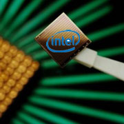 Intel's and the University of California's, Santa Barbara, researchers have developed the industry's first electrically powered Hybrid Silicon Laser using standard silicon manufacturing processes. This breakthrough addresses one of the last major barriers to producing low-cost, high-bandwidth silicon photonics devices for use inside and around future computers and data centers. The researchers were able to combine the light-emitting properties of Indium Phosphide with the light-routing capabilities of silicon into a single hybrid chip. When voltage is applied, light generated in the Indium Phosphide enters the silicon waveguide to create a continuous laser beam that can be used to drive other silicon photonic devices. A laser based on silicon could drive wider use of photonics in computers because the cost can be greatly reduced by using high-volume silicon manufacturing techniques. Intel's and the University of California's, Santa Barbara, researchers have developed the industry's first electrically powered Hybrid Silicon Laser using standard silicon manufacturing processes. This breakthrough addresses one of the last major barriers to producing low-cost, high-bandwidth silicon photonics devices for use inside and around future computers and data centers. The researchers were able to combine the light-emitting properties of Indium Phosphide with the light-routing capabilities of silicon into a single hybrid chip. When voltage is applied, light generated in the Indium Phosphide enters the silicon waveguide to create a continuous laser beam that can be used to drive other silicon photonic devices. A laser based on silicon could drive wider use of photonics in computers because the cost can be greatly reduced by using high-volume silicon manufacturing techniques.While widely used to mass produce affordable digital electronics today, silicon can also be used to route, detect, modulate and even amplify light, but not to effectively generate light. In contrast, Indium Phosphide-based lasers are commonly used today in telecommunications equipment. But the need to individually assemble and align them has made them too expensive to build in the high volumes and at the low costs needed by the PC industry. The hybrid silicon laser involves a novel design employing Indium Phosphide-based material for light generation and amplification while using the silicon waveguide to contain and control the laser. The key to manufacturing the device is the use of a low-temperature, oxygen plasma - an electrically charged oxygen gas - to create a thin oxide layer (roughly 25 atoms thick) on the surfaces of both materials. When heated and pressed together the oxide layer functions as a "glass-glue" fusing the two materials into a single chip. When voltage is applied, light generated in the Indium Phosphide-based material passes through the oxide "glass-glue" layer and into the silicon chip's waveguide, where it is contained and controlled, creating a hybrid silicon laser. The design of the waveguide is critical to determining the performance and specific wavelength of the hybrid silicon laser. The announcement builds on Intel's other accomplishments in its long-term research program to "siliconize" photonics using standard silicon manufacturing processes. In 2004, Intel researchers were the first to demonstrate a silicon-based optical modulator with a bandwidth in excess of 1GHz, nearly 50 times faster than previous demonstrations of modulation in silicon. In 2005, Intel researchers were the first to demonstrate that silicon could be used to amplify light using an external light source to produce a continuous wave laser-on-a-chip based on the "Raman effect". Bowers has worked with Indium Phosphide-based materials and lasers for more than 25 years. Currently his research is focused on developing novel optoelectronic devices with data rates as high as 160Gb/s and techniques to bond dissimilar materials together to create new devices with improved performance. write your comments about the article :: © 2006 Computing News :: home page |